- 您现在的位置:买卖IC网 > Sheet目录2001 > ISL5627INZ (Intersil)IC DAC DUAL 8BIT 3.3V 48-LQFP
11
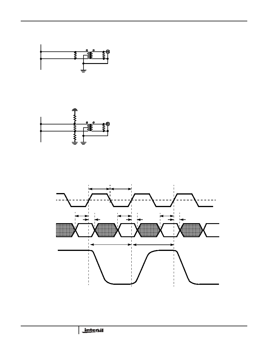
Propagation Delay
The converter requires two clock rising edges for data to be
represented at the output. Each rising edge of the clock
captures the present data word and outputs the previous
data. The propagation delay is therefore 1/CLK, plus <2ns of
processing. See Figure 8.
Test Service
Intersil offers customer-specific testing of converters with a
service called Testdrive. To submit a request, fill out the
Testdrive form at www.intersil.com/testdrive. Or, send a
request to the technical support center.
RDIFF
ISL5627
RLOAD
FIGURE 6. OUTPUT LOADING FOR DATASHEET
MEASUREMENTS
OUTA
OUTB
VOUT = (2 x OUTA x REQ)V
LOAD SEEN BY THE TRANSFORMER
RLOAD REPRESENTS THE
1:1
REQ = 0.5 x (RLOAD//RDIFF)
AT EACH OUTPUT
FIGURE 7. ALTERNATIVE OUTPUT LOADING
ISL5627
OUTA
OUTB
VOUT = (2 x OUTA x REQ)V
REQ = 0.5 x (RLOAD//RDIFF//RA), WHERE RA = RB
AT EACH OUTPUT
RLOAD
RDIFF
RA
RB
LOAD SEEN BY THE TRANSFORMER
RLOAD REPRESENTS THE
Timing Diagram
FIGURE 8. PROPAGATION DELAY, SETUP TIME, HOLD TIME AND MINIMUM PULSE WIDTH DIAGRAM
CLK
IOUT
50%
tPW1
tPW2
tSU
tHLD
tSU
tPD
tHLD
D7-D0
W0
W1
W2
W3
OUTPUT = W0
OUTPUT = W1
tPD
OUTPUT = W-1
ISL5627
发布紧急采购,3分钟左右您将得到回复。
相关PDF资料
ISL5629/2INZ
IC DAC 8BIT CMOS DUAL 48LQFP
ISL5727INZ
IC DAC DUAL 10BIT 3.3V 48-LQFP
ISL5729/2INZ
IC DAC 10BIT CMOS DUAL 48LQFP
ISL5757IBZ
IC DAC 10BIT 260MHZ 28-SOIC
ISL5761/2IBZ
CONV D/A 10BIT HS LP 28-SOIC
ISL5827INZ
IC DAC DUAL 12BIT 3.3V 48-LQFP
ISL5857IAZ
IC DAC 12-BIT 260MSPS 28-TSSOP
ISL5861/2IBZ
IC DAC 12BIT 210MSPS 28-SOIC
相关代理商/技术参数
ISL5629
制造商:INTERSIL 制造商全称:Intersil Corporation 功能描述:Dual 8-bit, +3.3V, 130/210MSPS, CommLink TM High Speed D/A Converter
ISL5629/2IN
功能描述:IC DAC DUAL 8BIT 3.3V 48-LQFP RoHS:否 类别:集成电路 (IC) >> 数据采集 - 数模转换器 系列:- 标准包装:2,400 系列:- 设置时间:- 位数:18 数据接口:串行 转换器数目:3 电压电源:模拟和数字 功率耗散(最大):- 工作温度:-40°C ~ 85°C 安装类型:表面贴装 封装/外壳:36-TFBGA 供应商设备封装:36-TFBGA 包装:带卷 (TR) 输出数目和类型:* 采样率(每秒):*
ISL5629/2INZ
功能描述:IC DAC 8BIT CMOS DUAL 48LQFP RoHS:是 类别:集成电路 (IC) >> 数据采集 - 数模转换器 系列:- 产品培训模块:Lead (SnPb) Finish for COTS
Obsolescence Mitigation Program 标准包装:1,000 系列:- 设置时间:1µs 位数:8 数据接口:串行 转换器数目:8 电压电源:双 ± 功率耗散(最大):941mW 工作温度:0°C ~ 70°C 安装类型:表面贴装 封装/外壳:24-SOIC(0.295",7.50mm 宽) 供应商设备封装:24-SOIC W 包装:带卷 (TR) 输出数目和类型:8 电压,单极 采样率(每秒):*
ISL56292IN
制造商:INTERSIL 制造商全称:Intersil Corporation 功能描述:Dual 8-bit, +3.3V, 130/210MSPS, CommLink TM High Speed D/A Converter
ISL5629EVAL1
功能描述:EVALUATION PLATFORM FOR ISL5629 RoHS:否 类别:编程器,开发系统 >> 过时/停产零件编号 系列:CommLink™ 标准包装:1 系列:- 传感器类型:CMOS 成像,彩色(RGB) 传感范围:WVGA 接口:I²C 灵敏度:60 fps 电源电压:5.7 V ~ 6.3 V 嵌入式:否 已供物品:成像器板 已用 IC / 零件:KAC-00401 相关产品:4H2099-ND - SENSOR IMAGE WVGA COLOR 48-PQFP4H2094-ND - SENSOR IMAGE WVGA MONO 48-PQFP
ISL5629IN
功能描述:IC DAC DUAL 8BIT 3.3V 48-LQFP RoHS:否 类别:集成电路 (IC) >> 数据采集 - 数模转换器 系列:- 标准包装:2,400 系列:- 设置时间:- 位数:18 数据接口:串行 转换器数目:3 电压电源:模拟和数字 功率耗散(最大):- 工作温度:-40°C ~ 85°C 安装类型:表面贴装 封装/外壳:36-TFBGA 供应商设备封装:36-TFBGA 包装:带卷 (TR) 输出数目和类型:* 采样率(每秒):*
ISL5629INZ
功能描述:IC DAC DUAL 8BIT 3.3V 48-LQFP RoHS:是 类别:集成电路 (IC) >> 数据采集 - 数模转换器 系列:- 产品培训模块:Lead (SnPb) Finish for COTS
Obsolescence Mitigation Program 标准包装:1,000 系列:- 设置时间:1µs 位数:8 数据接口:串行 转换器数目:8 电压电源:双 ± 功率耗散(最大):941mW 工作温度:0°C ~ 70°C 安装类型:表面贴装 封装/外壳:24-SOIC(0.295",7.50mm 宽) 供应商设备封装:24-SOIC W 包装:带卷 (TR) 输出数目和类型:8 电压,单极 采样率(每秒):*
ISL5640
制造商:INTERSIL 制造商全称:Intersil Corporation 功能描述:3V Dual 8-Bit, 20/40/60MSPS A/D Converter with Internal Voltage Reference